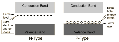
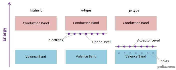
Energy Band Diagram P Type And N Type Semiconductor
Doped Semiconductors
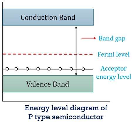
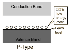
What Is P Type Semiconductor Energy Diagram And Conduction Circuit Globe
Draw The Energy Band Diagrams Of P Type And N Type Semiconductors A Semiconductor Has Equal Electron And Hole Concentration 6 X 10⁸ M 3 On Doping With A Certain Impurity Electron Concentration Increases To 8
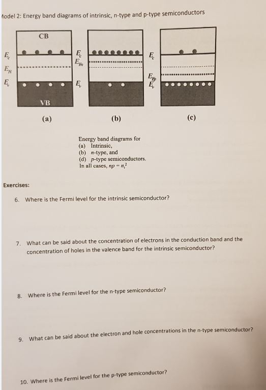
Solved Model 2 Energy Band Diagrams Of Intrinsic N Type Chegg Com

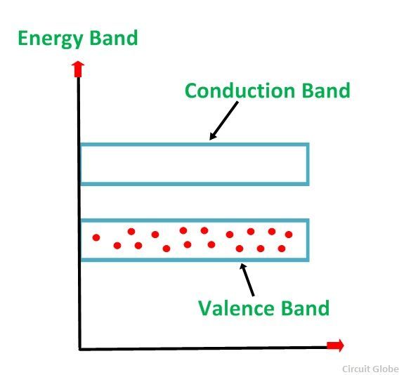
Energy Band Diagram Of P Type And N Type Semiconductor Youtube

Draw Energy Band Diagram Of P N Type Semiconductors Also Write


P N Junctions
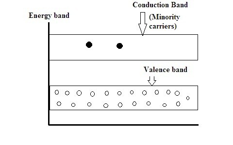
What Is P Type Semiconductor Energy Diagram Conduction Examples
Difference Between P Type And N Type Semiconductor With Comparison Chart Electronics Desk

Energy Band Diagram A Intrinsic Semiconductor B N Type Semiconductor Download Scientific Diagram

Extrinsic Semiconductors Dopants N Type P Type Semiconductor Q A

Extrinsic Semiconductors Dopants N Type P Type Semiconductor Q A
Doped Semiconductors

Draw Energy Band Diagram Of P Amp N Type Semiconductors Also Write Two Differences Between P And N Brainly In
18 P Type Semiconductor Electronic Circuits Part1 Semiconductors Youtube

Band Diagram For Activation Energy In P Type Semiconductor Download Scientific Diagram

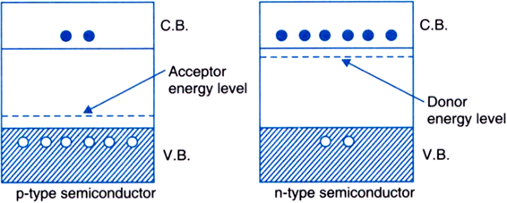
Draw The Energy Band Diagram Of I N Type And Ii P Type Semiconductors At Temperature T 0 K In The Case Of N Type Si Semiconductor The Donor Energy Level Is Slightly Below The Bottom Of Conduction Band Whereas

Draw Energy Band Diagram For N Type Semiconductor P Type Semiconductor Physics Semiconductor Electronics Materials Devices And Simple Circuits 9818193 Meritnation Com
Draw The Energy Band Diagrams Of I N Type And Ii P Type Semiconductor At Temperature Sarthaks Econnect Largest Online Education Community
Difference Between P Type And N Type Semiconductor
Source : pinterest.com